Elemental technologies
Mechatronics, Machine vision and Ultrasonic technology to support your production.
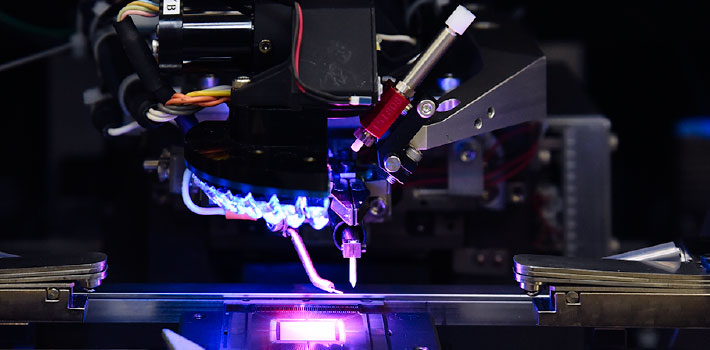
One of the reasons for choosing KAIJO as a production partner is our wide range of 'Elemental
technologies'. We have a long history of R&D and hope that these elemental technologies will
support the next generation of industry.
Mechatronics and Machine vision technology
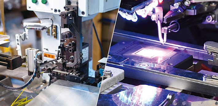
KAIJO uses the mechatronics and machine vision technology know-how it has acquired through the
development of semiconductor equipment to propose in-line systems that are optimised for
customer production.
< Mechatronics >
Technology for automatic production lines with high-speed, high-precision control.It significantly
reduces the time required for assembly, improves productivity and stabilises quality.
< Machine vision >
High-precision positioning technology based on ultra-high-speed image recognition.Positioning of
even small workpieces in less than 0.1s (1/10th of a second) is possible.High-precision fail
judgement is also possible using image recognition.
Bonding technology for dissimilar materials
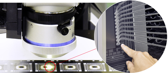
The ultrasonic bonding technology that KAIJO has acquired in the development of semiconductor
machines is applied to a wide range of applications. We are expanding our research into materials
other than metal bonding.
Ultrasonic wire bonders are used in the manufacture of semiconductor devices in the process of joining IC chip electrodes and leadframes with metal wires. Ultrasonic can be used to bond objects without
melting them. This technology is also used to bond between different materials.
Solid-state bonding
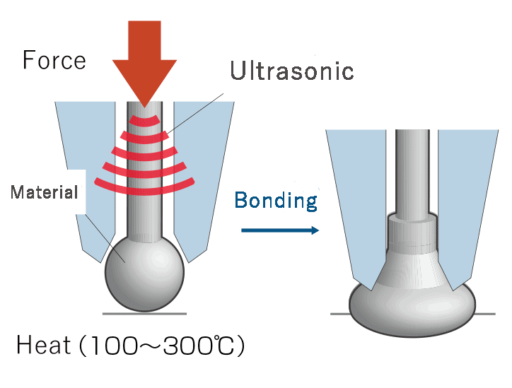
Methods of bonding metals without melting.
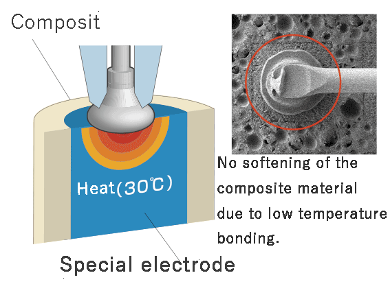
Low temperature bonding is possible even with non-heat resistant materials.
Bonding technology for ultra-fine wire
The connecting electrodes formed on semiconductor chips or wiring leads are called bumps, which
require bonding technology using, for example, 15 µm gold wire at a pitch of 35 µm. The shape of the
bump tip can be processed and this know-how can be applied in other fields.
Ultra-fine bump bonding
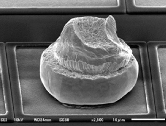
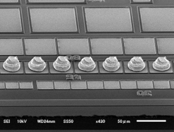
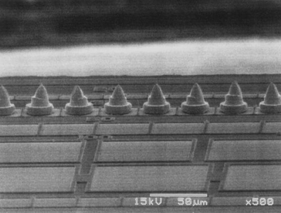
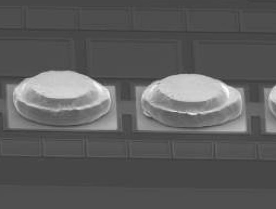
Ultra-fine wire bonding
This is an example of fine pitch bonding using ultra-fine wire.
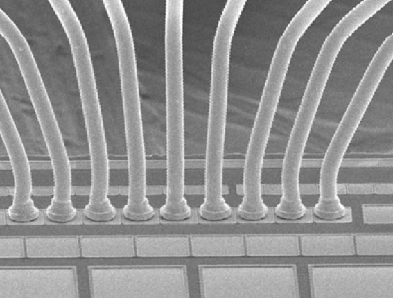
PDA pitch 30μm
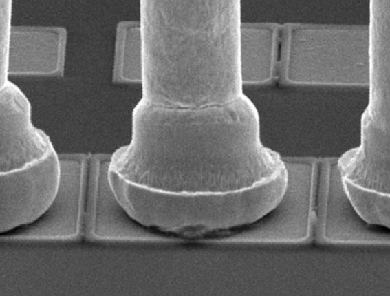
Enlarged view (wireφ 12.5µm)
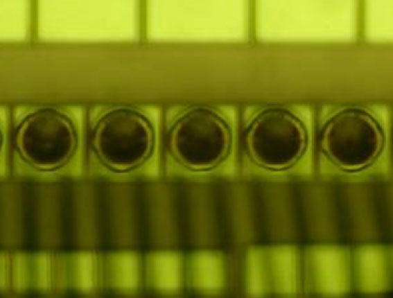
Whole image
Applied to electrode
An example of electrode joining with platinum. Size can be up to the equivalent of 4 times the wire diameter. The sphere size at the tip can be adjusted by setting.
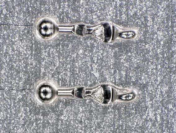
e.g. 1
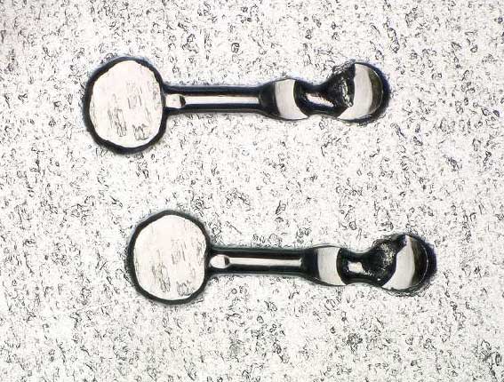
e.g. 2
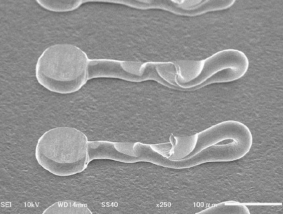
e.g. 3
Bonding technology for insulated coated wires
KAIJO has bonding technology with polyurethane coatings. We have expertise in micro-bonding and have applied for a process patent for the technology to remove the coating by ultrasonic. This reduces the amount of soldering work that used to be carried out manually, saving manpower and realising automation.
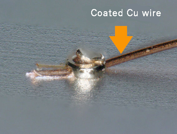
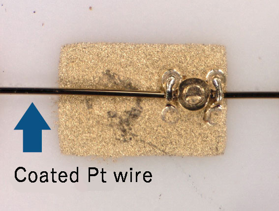
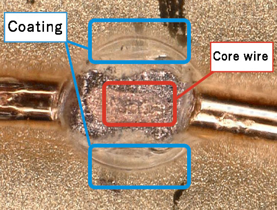
Enlarged top view
Flexible wiring technology
KAIJO has a wide variety of highly flexible wiring technologies developed in electrode-to-electrode connections. For example, it is possible to form 'chain loops' with ultra-fine wires.
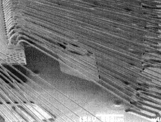
Staggered wiring
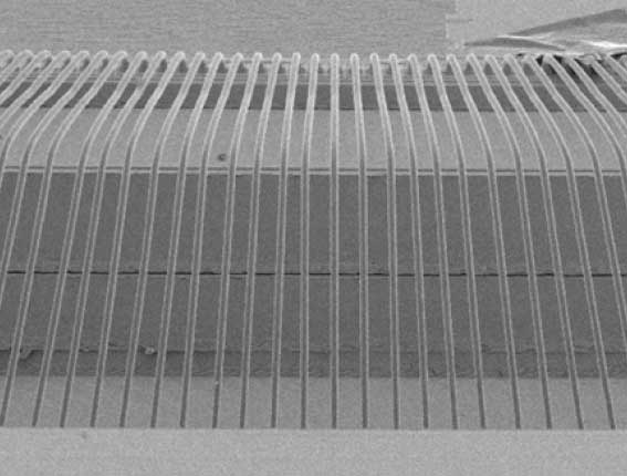
Large gap
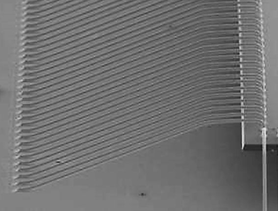
Overhang
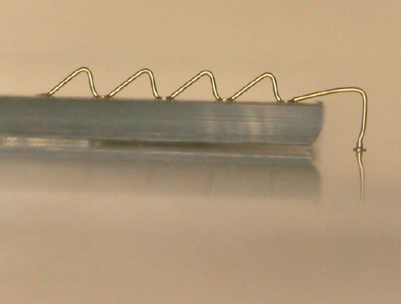
Chain loop
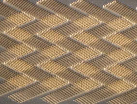
Wiring flexibility
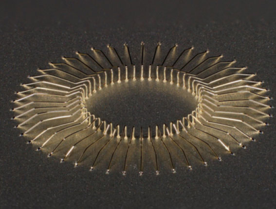
High accurate repeatability
Even if you are just at the idea stage,Please do not hesitate to contact us.
- Contact InformationInquiries about products
- Please contact us for technical inquiries and technical information from here.